Errors in the Definitive Guide for ARM Cortex-M book series
Embarrassing to say, but just like any other technical documentation, there are a few errors in my Arm Cortex-M books. In this document I summarize the errors I am aware of.
By Joseph Yiu

Embarrassing to say, but just like any other technical documentation, there are a few errors in my books on Arm Cortex-M. Over the years I have learn a lot from my mistakes, but it is still impossible to catch all of the errors before the books are printed. In this document I summarize the errors I am aware of. This document will be updated from time to time as and when issues are found.
I hope you enjoy the books.
regards,
Joseph
Note: The page numbers are referring to the pages on paper copies. Some of the errors spotted in the early version of the the book are already fixed in some of the newer prints / electronic copies.
Definitive Guide to Arm Cortex-M23 and Cortex-M33 Processors, 1st edition
| Page | Descriptions | ||||||||||||||||||
| 86 |
Figure 4.1 "Cortex-4" should be "Cortex-M4" |
||||||||||||||||||
| 98 |
Typo near top of the page "The PRIMASK, FAULTMASK, and BASEPRI registers:" PRIMARK -> PRIMASK |
||||||||||||||||||
| 99 |
Typo in the code near top of the page (PRIMARK -> PRIMASK): x = __get_BASEPRI(); // Read BASEPRI register |
||||||||||||||||||
| 100 |
Table 4.4 Two typos in SPSEL description: "Stack Pointer select - Selects between Main Stack Pointer (MSP) or Process Stack Pointer (PSP) in Thread mode: - If this bit is 0 (default), the MSP is selected. - if this bit is 1, the PSP is selected. In Handler mode, the MSP is always selected and this bit is 0 - writing to this bit is ignored." |
||||||||||||||||||
| 110 |
Section 4.2.4 Typo in the following line: "-Secure stack pointers (MPS_S, PSP_S)" MPS_S should be MSP_S. |
||||||||||||||||||
| 113 |
Section 4.3.1 Memory Map By default, the 4GB address space of Cortex-M processors is partitioned into a number of memory regions, as shown in Fig. 4.21. should be By default, the 4GB address space of Cortex-M processors is partitioned into a number of memory regions, as shown in Fig. 4.19. |
||||||||||||||||||
| 162 |
Table 5.22, last row. "Read" should be "Write".
|
||||||||||||||||||
| 163 |
Table 5.23, last 3 rows. "Read" should be "Write".
|
||||||||||||||||||
| 178 |
Table 5.38, first row.
Third row
|
||||||||||||||||||
| 191 |
Table 5.47. In SXTH and UXTH, "byte" should be "half word"
|
||||||||||||||||||
| 192 |
Table 5.48. In SXTH and UXTH, "byte" should be "half word", and the source register bit fields for the UXTH instruction are incorrect. The correct descriptions are as follow:
|
||||||||||||||||||
| 205 |
Table 5.60, first row (table header), "true" should be "then" IT block (each of <x>, <y> and <z> can either be T (then) or E (else) |
||||||||||||||||||
| 207 |
Figure 5.18. Typo in the label on top left "PC (address of the TBB instruction)" should be "PC (address of the TBH instruction)" |
||||||||||||||||||
| 220 |
Typo in 5.16.2 : CPACR Address in the following bullet "0xE002ED880" should be "0xE002ED88" The Non-secure version of the CPACR can be accessed by both Secure and Non-secure |
||||||||||||||||||
| 223 |
Table 5.72 "Accumulate" in the description of VNMLS should be Subtract.
|
||||||||||||||||||
| 234 |
Table 5.80 Description of MCRR and MCRR2 is incorrect. It should be "Transfers 64 bits from two processor registers to a coprocessor register (opcode 1 is 4 bits)" |
||||||||||||||||||
| 255 |
Table 6.4 For "Devices (0xC0000000 - 0xDFFFFFFF)", the second column (Memory/Device type) should be "Device-nGnRE". |
||||||||||||||||||
| 309 |
8.4.3 (above starting of 8.4.4) The PC would also be updated to the starting address of the exception handler and the LR would be updated with a special value, called |
||||||||||||||||||
| 324 |
Table 8.12 Missing “Non-secure” in the register name in the last row:
|
||||||||||||||||||
| 342 |
Middle of the page "As shown in Table 9.3, the IRQn_Type uses negative values for system exceptions, value zero and positive values for interrupts." (Technically 0 is not classified as a positive number hence the correction). |
||||||||||||||||||
| 350 |
Last paragraph above table 9.10. Copy and paste error: "CMSIS-CORE provides the following functions for accessing the Interrupt Target Non-secure registers:" |
||||||||||||||||||
| 354 |
Table 9.15 System Handler Priority Registers:Register symbol SHP should be SHPR. SCB->SHP[0] to SCB->SHP[1] or SCB->SHP[11] should be SCB->SHPR[0] to SCB->SHPR[1] or SCB->SHPR[11] ------ "Handle" -> "Handler" in SHCSR description 0xE000ED24 | System Handler Control and State Register | SCB->SHCSR | For controlling fault exceptions (e.g., enable / disable) and for the status of system exceptions. |
||||||||||||||||||
| 355 |
Section 9.3.3 heading: System Handler Priority Registers (SCB->SHB[n]) should be System Handler Priority Registers (SCB->SHBR[n]) |
||||||||||||||||||
| 362 |
Typo (PRIMARK -> PRIMASK) in the following: "Please note, the masked priority levels of the Non-secure PRIMASK_NS, FAULTMASK_NS, and BASEPRI_NS (is) are affected by the PRIS (Prioritize Secure Exceptions) |
||||||||||||||||||
| 363 |
In the following paragraph in section 9.4.1: "When using interrupt masking registers when writing software, instead of just setting an "read-modify-write" should be changed to "save-operate-restore". |
||||||||||||||||||
| 385 |
Section 10.2.3, typo in 4th paragraph: "SCB_NS->SCB" should be "SCB_NS->SCR" "When TrustZone is implemented, Secure privileged software is also able to access the Non-secure privileged view of this register using SCB_NS->SCR (address 0xE002ED10)." |
||||||||||||||||||
| 402 |
10.4.2.6 Ambiguous sentence: "For example, if you use a voltage source with a higher voltage than required you will need to reduce the voltage and, by so doing, often waste power." should be changed to: "For example, if you use a voltage source with a higher voltage than required, you will need to reduce the voltage. Otherwise, the system could be wasting power." |
||||||||||||||||||
| 403 |
10.4.2.10: "Skew" should be "slew" "Some microcontrollers have programmable I/O port options to control the drive strength (i.e. the electrical current supported by the I/O pins on the chip) and the slew rate. Depending on the devices connected to the I/O pins, the power consumption of the I/O interface logic can be reduced by having a lower drive strength or a slower slew rate configuration. " |
||||||||||||||||||
| 405 |
Table 10.7 fourth row SCB->SHP[n] should be SCB->SHPR[n] ------ Table 10.7 last row The register name should be System Handler Control and State Register, |
||||||||||||||||||
| 407 |
Table 10.8 SCB->SHP[n] should be SCB->SHPR[n] |
||||||||||||||||||
| 412 |
Section 10.5.5.3 Typo in CCR - BFHFNMIGN bit description "MemMenage fault" should be "MemManage fault" |
||||||||||||||||||
| 414 |
Table 10.13, description for EXTEXCLALL - Only value of 0 is the default. Value of 1 isn't. "When this bit is 0 (default), only the exclusive access to the sharable memory can utilize the exclusive access sideband signals (this enables the use of a global exclusive access monitor, see Section 6.7). |
||||||||||||||||||
| 414 |
Table 10.13 Row 4 (below EXTEXCLALL): bit 38:13 should be 28:13 |
||||||||||||||||||
| 425 |
Section 11.2.3.4 Typo in code. ("!=" should be "==" in the line that "Waits until the SysTick is reloaded) unsigned int start_time, stop_time, cycle_count; |
||||||||||||||||||
| 430 |
Section 11.3.3, there is a typo in the 2nd bullet, MSP should be PSP: “In devices where there are multiple RAM regions that are not continuous you can configure the thread stack (using PSP) to one RAM region and the Handler stack to another.” |
||||||||||||||||||
| 434 |
Table 11.9 Several typos in the descriptions. Corrected version below:
|
||||||||||||||||||
| 464 |
"Translation Lookup Buffer (TLB)" should be "Translation Lookaside Buffer (TLB)" |
||||||||||||||||||
| 471 |
Section 12.2.5, typo in Non-shareable description: Non-shareable: An update of data in a Non-shareable region by CPU #0 is not always |
||||||||||||||||||
| 508 |
Near top of the page, there is missing text in the last bullet: "Lockups can occur if:
|
||||||||||||||||||
| 526 |
Section 14.2.2 In the sentence below, Fig. 14.3 should be Table 14.3. When the TrustZone® security extension is implemented, Secure software has access to the Non-secure view of those registers, listed in Table 14.3, via the Non-secure address alias 0xE002Exxx. |
||||||||||||||||||
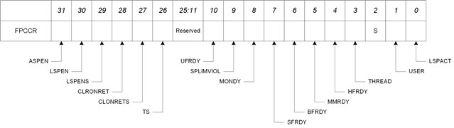
| 532 |
Figure 14.15: Bit 6 (BFRDY) is missing from the figure.
|
||||||||||||||||||
| 533 |
Section 14.2.7, Table 14.8 FPCCR description. Description of TS (Treat as Secure) bit unclear. Improved version as follows:
|
||||||||||||||||||
| 535 |
Section 14.2.7, Table 14.8 FPCCR description. The description of S (bit S) has one issue - type should be R (read only) The description of USER (bit 1) has two issues:
|
||||||||||||||||||
| 542 |
Beginning of section 14.4.4. "interrupt code" should be "interrupted code" "If the interrupted code has a floating-point context and there is a floating-point operation inside the ISR, the deferred lazy stack process has to be carried out. ...." |
||||||||||||||||||
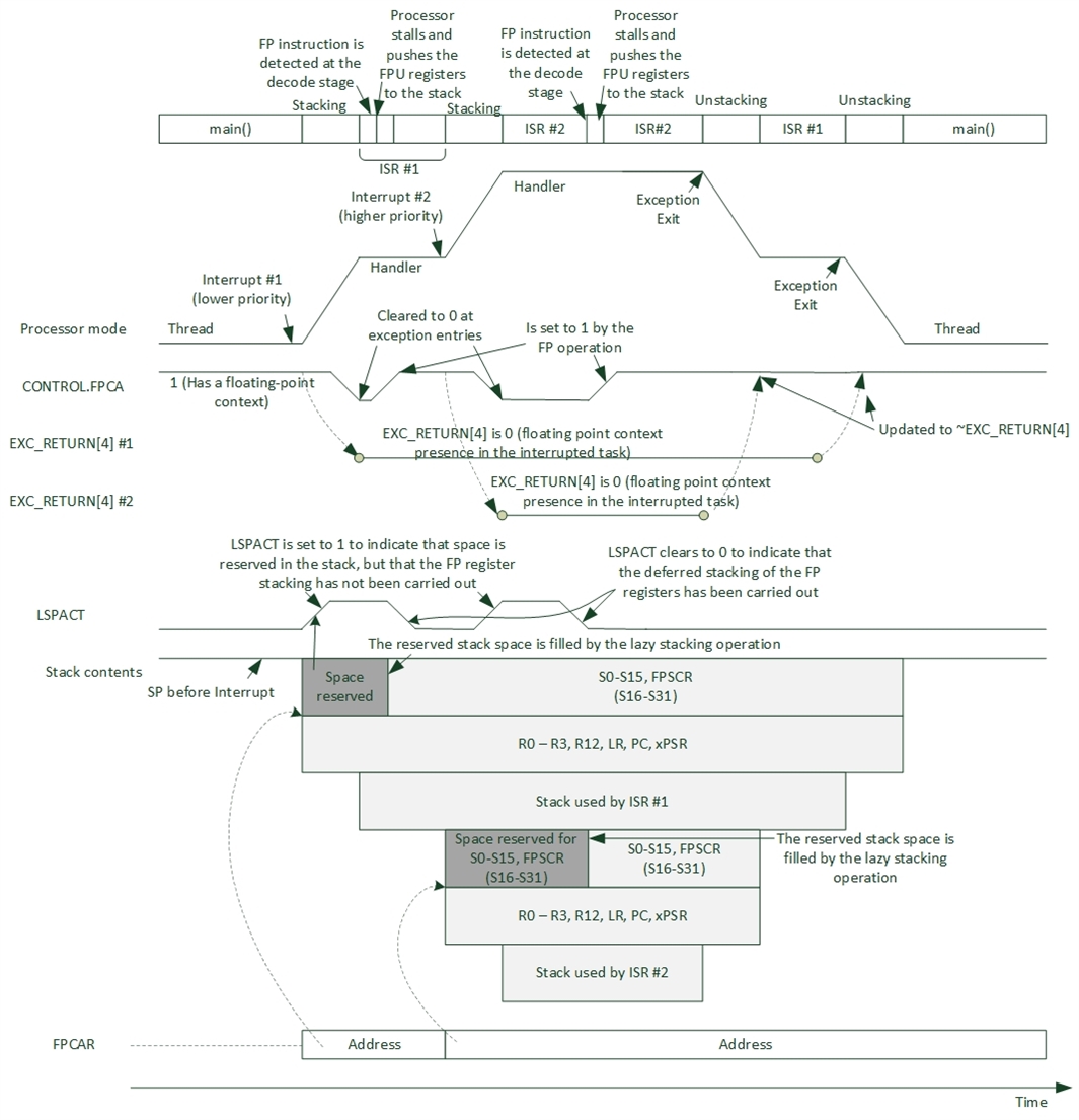
| 546 |
Figure 14.24 Error in the CONTROL.FPCA after the exception return of the higher priority interrupt. The value of this bit should stay high because the first ISR has previously used the FPU. The correct diagram is shown below.
|
||||||||||||||||||
| 607 |
Table 16.18: Incorrect prefix for register symbols for two registers.
|
||||||||||||||||||
| 617 |
Table 16.31: Incorrect Non-secure alias address for ITM Trace Control Register and
|
||||||||||||||||||
| 619 |
Typo in the following text (unit32_t should be uint32_t) : To assist software development, the CMSIS-CORE provides a function, as detailed below,
|
||||||||||||||||||
| 744 |
In the example code in section 18.6.5.1 The comments in the following code segment w swapped.
|
The Definitive Guide to ARM Cortex-M3 and Cortex-M4 Processors, 3rd edition
| Page | Descriptions | ||||||||||||||||||||||||||||||||||||||||
|---|---|---|---|---|---|---|---|---|---|---|---|---|---|---|---|---|---|---|---|---|---|---|---|---|---|---|---|---|---|---|---|---|---|---|---|---|---|---|---|---|---|
| 4 |
Typo at bottom of page: "Intellectualy Property" should be "Intellectual Property" |
||||||||||||||||||||||||||||||||||||||||
| 10 | Typo near bottom of page: "a wide range of coins on software development/debug tools" should be "a wide range of choices on software development/debug tools" | ||||||||||||||||||||||||||||||||||||||||
| 38 | Near bottom of page: "A timer is need to" should be "A timer is needed to" | ||||||||||||||||||||||||||||||||||||||||
| 80 |
Bottom of the page: "the setting of LSB in branch targets is handled by the compiler automatically" should be "the setting of LSB in branch targets is handled by the development toolchain automatically" (Note: In some tool chains this is handled by linker, and in some cases, e.g. gcc, the compiler invoke the linker and therefore the linking stage is hidden. So it is better to generalize by stating the toolchain handle this automatically.) |
||||||||||||||||||||||||||||||||||||||||
| 83 |
Typo at middle of page ("ERSR" should be "EPSR"): The EPSR cannot be accessed by software code directly using MRS (read as zero) or MSR |
||||||||||||||||||||||||||||||||||||||||
| 94 |
Table 4.7, second row 0x90000000 + 0x90000000, result should be 0x20000000 (not 0x30000000) |
||||||||||||||||||||||||||||||||||||||||
| 95 | The statement "In most cases, the instructions for saturation arithmetic are mnemonic starting with “Q,” for example “QADD16". If saturation occurred, the Q bit is set; otherwise, the value of the Q bit is unchanged." is inaccurate. The list of instruction that can set Q bit are QADD, QDADD, QSUB, QDSUB, SSAT, SSAT16, USAT, USAT16. Some other instructions start with Q (QADD8, QADD16, QASX, QSUB8, QSUB16, QSAX) and all instructions starting with UQ (UQADD8, UQADD16, UQSUB8, UQSUB16, UQASX, UQSAX) do not change the Q bit. Therefore the statement should be changed to: "In most cases, the instructions for saturation arithmetic are mnemonic starting with “Q,” for example “QADD16". If saturation occurred, the Q bit is set for the following instructions - QADD, QDADD, QSUB, QDSUB, SSAT, SSAT16, USAT, USAT16; otherwise, the value of the Q bit is unchanged." |
||||||||||||||||||||||||||||||||||||||||
| 95 |
4.3.3, first paragraph (or -> of) For SIMD instructions with 16-bit data, bit 0 and bit 1 are controlled by the result of lower half-word, and bit 2 and bit 3 are controlled by the result of upper half-word. |
||||||||||||||||||||||||||||||||||||||||
| 100 |
Figure 4.20, the order of POP instructions should be inverted of the order in PUSH. The corrected diagram is shown below:  |
||||||||||||||||||||||||||||||||||||||||
| 108 |
Figure 4.26: Value in address 0x00 "Initial value of MPS" should be "Initial value of MSP" Figure 4.26: Typo on BusFault row, exception type should be 5, not 4. |
||||||||||||||||||||||||||||||||||||||||
| 126 |
Table 5.1: The directive for inserting instructions in GNU Assembler should be ".inst / .inst.n / .inst.w E.g., .inst.n 0xBE00" |
||||||||||||||||||||||||||||||||||||||||
| 132 | MVN description: Should be "Move NOT" rather than "Move negative" | ||||||||||||||||||||||||||||||||||||||||
| 135 |
In the paragraph under table 5.6 For example, if 0x83 is read in a LDRSB instruction, the value is converted into 0xFFFFFF83 before being placed in the destination register. |
||||||||||||||||||||||||||||||||||||||||
| 136 |
In the third paragraph in page 136 it should be "If the floating point unit is present, the instructions in Table 5.10 are also available to perform LDR and STR operations to the registers in the floating point unit." |
||||||||||||||||||||||||||||||||||||||||
| 136 |
On Page 136, in the third paragraph, "cannot be used with R15(PC) or R14(SP)." should be "... or R13(SP)." |
||||||||||||||||||||||||||||||||||||||||
| 139 |
On Page 139, in the fourth paragraph, "cannot be used with R15(PC) or R14(SP)." should be "... or R13(SP)." |
||||||||||||||||||||||||||||||||||||||||
| 141 |
Table 5.16: The text in the description column reference "Rd", instead of "Rn". |
||||||||||||||||||||||||||||||||||||||||
| 141, 142 |
Table 5.17, first column header "Example of Stack Operation" should be "Example of Multiple Load / Store for FPU registers". |
||||||||||||||||||||||||||||||||||||||||
| 149 |
Table 5.24, errors in comments for last two EOR instructions in the table EOR Rd, Rn,#immed ; Rd = Rn ^ #immed EOR Rd, Rn, Rm ; Rd = Rn ^ Rm |
||||||||||||||||||||||||||||||||||||||||
| 151 |
REV16 mistyped as REVH: REV reverses the byte order in a data word, and REV16 reverses the byte order inside a half-word. For example, if R0 is 0x12345678, in executing the following: REV R1, R0 REV16 R2, R0 R1 will become 0x78563412, and R2 will be 0x34127856 |
||||||||||||||||||||||||||||||||||||||||
| 152 |
REV16 mistyped as REVH: REVSH is similar to REV16 except that it only processes the lower half-word and then sign extends the result. For example, if R0 is 0x33448899, running: REVSH R1, R0 R1 will become 0xFFFF9988. |
||||||||||||||||||||||||||||||||||||||||
| 153 |
Example for RBIT does not match descriptions: For example, if R0 is 0xB4E10C23 (binary value 1011_0100_1110_0001_0000_1100_0010_0011), executing: RBIT R0, R0 R0 will become 0xC430872D (binary value 1100_0100_0011_0000_1000_0111_0010_1101). |
||||||||||||||||||||||||||||||||||||||||
| 154 |
Table 5.30, error in the operation descriptions in last two rows (AND should be XOR) TEQ <Rn>, <Rm> Test (bitwise XOR): Calculate XOR result between Rn and Rm. N bit and Z bit in APSR are updated but the XOR result is not stored. C bit can be updated if barrel shifter is used. TEQ <Rn>, #<immed> Test (bitwise XOR): Calculate XOR result between Rn and immediate data. N bit and Z bit in APSR are updated but the XOR result is not stored |
||||||||||||||||||||||||||||||||||||||||
| 158 |
Table 5.35 ("then" should be "than") GT Signed greater than Z flag is cleared, and either both N flag and V flag are set, or both N flag and V flag are cleared (Z == 0 and N == V) |
||||||||||||||||||||||||||||||||||||||||
| 176 |
Table 5.49 Foot note 2 "Q bit is set when saturation occurs" is incorrect. This should be corrected to "These instructions do not set Q bit." |
||||||||||||||||||||||||||||||||||||||||
| 178, 179 |
Table 5.53 Q bit is not set for the following instructions: QADD8, QADD16, QASX, QSUB8, QSUB16, QSAX, UQADD8, UQADD16, UQSUB8, UQSUB16, UQASX, UQSAX |
||||||||||||||||||||||||||||||||||||||||
| 204 |
Table 6.6 Data on AHB bus for ARM7TDMI
|
||||||||||||||||||||||||||||||||||||||||
| 216 |
Typo in BITBAND macro in the bottom of the page #define BIT BAND(addr,bitnum) ((addr & 0xF0000000)+0x02000000+((addr & 0xFFFFF)<<5)+(bitnum<<2)) |
||||||||||||||||||||||||||||||||||||||||
| 218 to 219 |
Section 6.9 Memory access attributes Last sentence in page 218 should be "The Cacheable and Bufferable attributes are usually used by a cache controller, which specifies memory types and caching scheme, as shown in Table 6.11." |
||||||||||||||||||||||||||||||||||||||||
| 247 | Figure 7.14 - "Entering the interrupt handler cause the active status to beset" should be "Entering the interrupt handler causes the active status to be set" | ||||||||||||||||||||||||||||||||||||||||
| 253 |
Table 7.9 CMSIS-Core symbol for Interrupt Priority Registers should be "IP", not "IR" NVIC->IP[0] to NVIC->IP[239] |
||||||||||||||||||||||||||||||||||||||||
| 261 |
Table 7.17 Width of VECTPENDING and VECTACTIVE incorrect. 20:12 VECTPENDING 8:0 VECTACTIVE Bit 21 and bit 9 are reserved. (Same issue for page e130, table F.9) |
||||||||||||||||||||||||||||||||||||||||
| 265 |
7.10.1 PRIMASK Typo near middle of the page: "PRIMARK" should be "PRIMASK" "In assembly language programming, you can change the value of PRIMASK register using CPS (Change Processor State) instructions:" |
||||||||||||||||||||||||||||||||||||||||
| 306 |
Errors in exclusive access example code for CMSIS-CORE - No need to have "&" in front of variable when using __LDREX and __STREX functions. For example, __LDREXW(&Lock_Variable) should have been __LDREXW(Lock_Variable) and status = __STREXW(1, &Lock_Variable);should have been status = __STREXW(1, Lock_Variable); |
||||||||||||||||||||||||||||||||||||||||
| 315 |
Table 9.8, reset value of SysTick Reload Value Register, and table 9.9, reset value of SysTick Current Value Register: In the architecture definition (ARMv7-M), the reset value of these two registers are unknown. However, in the actual implementation (in the current Cortex-M3 and Cortex-M4 processor designs), these two registers are reset to 0. Therefore the reset values in these two table should be changed to unknown, with a footnote added to these two tables : " * Architecturally the reset values is unknown, but in actual processor design the register is reset as 0. But this is not guarantee that it will be the same in future versions." |
||||||||||||||||||||||||||||||||||||||||
| 329 |
Typo in comments in example code (near middle of page) "ISB ; Execute and ISB after updating CONTROL" should be "ISB ; Execute an ISB after updating CONTROL" |
||||||||||||||||||||||||||||||||||||||||
| 335 |
In example code B __cpp(SVC_Handler_C) should have been B __cpp(SVC_Handler_main) |
||||||||||||||||||||||||||||||||||||||||
| 336 |
"For a system with only two tasks, the two tasks are executed alternatively, as shown in Figure 10.6." should be "For a system with only two tasks, the two tasks are executed alternately, as shown in Figure 10.6." |
||||||||||||||||||||||||||||||||||||||||
| 335 |
SVC with priority escalation lead to HardFault, not Usage Fault. "Because of the exception priority model, you cannot use SVC inside an SVC handler (because the priority us the same as the current priority). Doing so will result in a HardFault exception. For the same reason, you cannot use SVC in the NMI handler or the HardFault handler." |
||||||||||||||||||||||||||||||||||||||||
| 356 |
"If the MPU is not enabled, the processor no MPU is present." should be "If the MPU is not enabled, it behaves as the processor has no MPU." |
||||||||||||||||||||||||||||||||||||||||
| 372 |
In C example, function "mpu_enable(uint32_t options)", there is a typo in the comment void mpu_enable(uint32_t options) { MPU->CTRL = MPU_CTRL_ENABLE_Msk j options; // Enable the MPU __DSB(); // Ensure MPU settings take effects __ISB(); // Sequence instruction fetches using update settings return; } |
||||||||||||||||||||||||||||||||||||||||
| 375 |
Figure 11.6. Text in diagram has incorrect SRD values: Task A's SRD should be 11100000 Task B's SRD should be 00000011 |
||||||||||||||||||||||||||||||||||||||||
| 377 |
Table 11.2, Clarification in "Registers accesses" Please note that in Cortex-M7 processors, the MPU registers are word access only. Half word and Byte accesses are supported in Cortex-M3 and Cortex-M4 but this is not an architectural requirement. |
||||||||||||||||||||||||||||||||||||||||
| 384 |
The Usage Fault exception can be caused by a wide range of factors: "Execution of SVC when the priority Level of the SVC is the same or lower than current Level " this scenario lead to a HardFault not a Usage Fault. |
||||||||||||||||||||||||||||||||||||||||
| 389 |
Section 12.4.5, first sentence should be: "The programmer's model for the HardFault Status Register is shown in Table 12.6." |
||||||||||||||||||||||||||||||||||||||||
| 403 |
the code at the top:
mrseq r0, msp mrseq r0, psp
should be:
mrseq r0, msp mrsne r0, psp |
||||||||||||||||||||||||||||||||||||||||
| 423 |
Section 13.2, table 13.7 FPCCR description. The description of USER (bit 1) has two issues:
|
||||||||||||||||||||||||||||||||||||||||
| 425 |
Section 13.2.8, typo in 2nd paragraph: FPFSCR should be FPDSCR. |
||||||||||||||||||||||||||||||||||||||||
| 449 |
Typo near bottom of the page: "For readers who would like to have a brief verview" -- should be overview. |
||||||||||||||||||||||||||||||||||||||||
| 455 |
Figure 14.7 Second block on the botton left should be labelled ITM, not DWT. |
||||||||||||||||||||||||||||||||||||||||
| 480 | Figure 14.20, typo in labels "Asynchornous FIFO" should be "Asynchronous FIFO". | ||||||||||||||||||||||||||||||||||||||||
| 482 |
Table 14.9, PID0 value in ROM table 0xC3 is only valid for Cortex-M3, For Cortex-M4 it is 0xC4. |
||||||||||||||||||||||||||||||||||||||||
| 656 |
First line of section "20.4.3 Accessing special registers" contains outdated information: "In the GNU toolchain, when accessing the special registers in assembly code, the name of the special registers must be in lower case". This is no longer the case, and has been fixed since 2007. See: Paul Brook - ARM uppercase MSR names Therefore the text should be changed to : "In recent version of the GNU toolchain, when accessing the special registers in assembly code, the name of the special registers can be in ether lower case or upper case, but not a mixture of lower/upper case." |
||||||||||||||||||||||||||||||||||||||||
| 668 |
gcc inline assembly section - bottom of the page. "In the code example, %0 is the first input parameter and %1 is the first output parameter." This sentence should be changed to "In the code example, %0 is the output parameter and %1 is the input parameter." More discussions about this error is here. |
||||||||||||||||||||||||||||||||||||||||
| 718 |
Section 22.3, typo in description of q7
|
||||||||||||||||||||||||||||||||||||||||
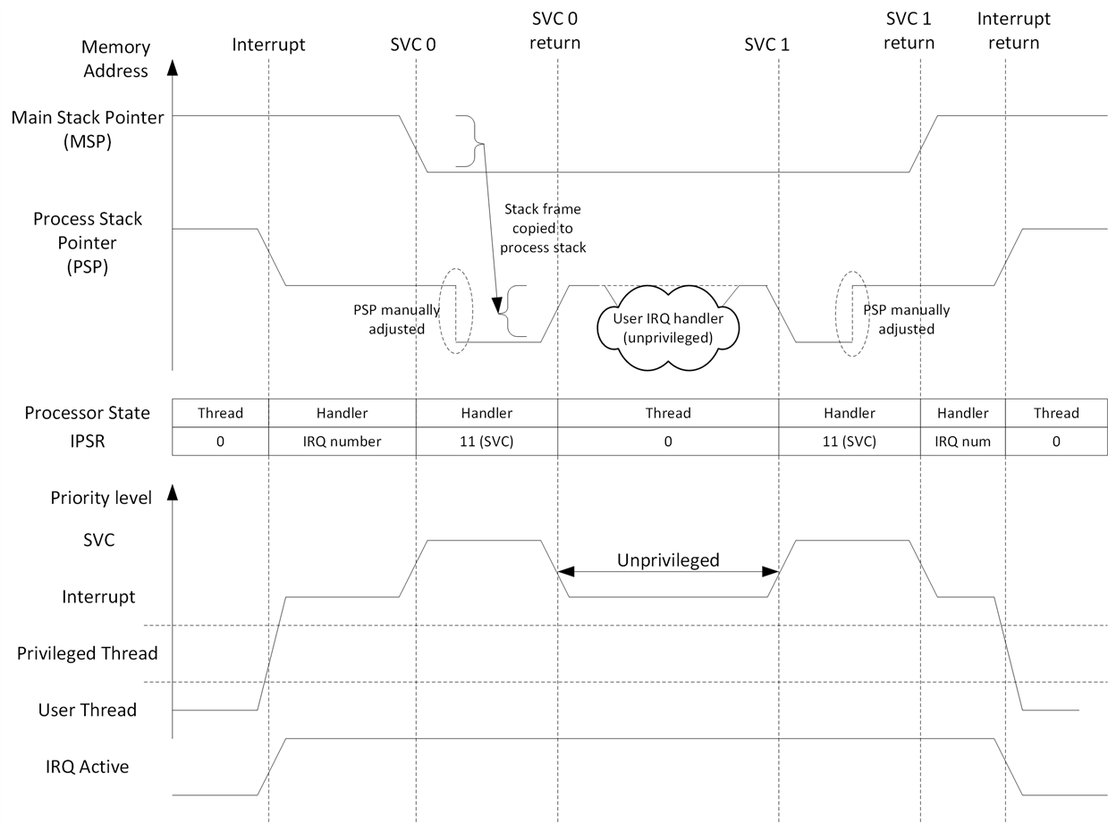
| 751 |
The illustration in Figure 23.4 mistakenly showing priority level of user (unprivileged) interrupt handler execute at user thread. While it is execute at user permission, priority level should be the same as the interrupt.
|
||||||||||||||||||||||||||||||||||||||||
| 754 |
Example for re-entrant interrupt handler. Two addition steps might be needed 1) to prevent a new re-entrant interrupt being triggered just before execution of SVC (I am still doing more check in this). To avoid the potential issue, set BASEPRI to the same level as the re-entrant interrupt (e.g. SysTick in this case) before SVC and clear BASEPRI inside the SVC Handler: 2) for Cortex-M4 with FPU, also need to trigger the deferred lazy stacking __asm void SysTick_Handler(void) { #if (__CORTEX_M >= 0x04) #if (__FPU_USED == 1) ; The following 3 lines are for Cortex-M4 with FPU only TST LR, #0x10 ; Test bit 4, if zero, need to trigger stacking IT EQ VMOVEQ.F32 S0, S0 ; Trigger lazy stacking stacking #endif #endif ; Now we are in Handler mode, using Main Stack, and ; SP should be Double word aligned MRS R0, PSR PUSH {R0, LR} ; Need to save PSR and LR in stack ... SysTick_Handler_thread_pt BL __cpp(Reentrant_SysTick_Handler) ; Block SysTick from being triggered just before SVC LDR R0,=0xE000ED23 ; Address of SysTick priority level LDR R0,[R0] MSR BASEPRI, R0 ; Block SysTick from being triggered ISB ; Instruction Synchronisation Barrier SVC 0 ; Use SVC to return to original Thread B . ; Should not return here __asm void SVC_Handler(void) { MOVS R0, #0 MSR BASEPRI, R0 ; Enable SysTick again ISB ; Instruction Synchronisation Barrier #if (__CORTEX_M >= 0x04) #if (__FPU_USED == 1) ; The following 3 lines are for Cortex-M4 with FPU only TST LR, #0x10 ; Test bit 4, if zero, need to trigger stacking IT EQ VMOVEQ.F32 S0, S0 ; Trigger lazy stacking stacking #endif #endif ; Extract SVC number TST LR, #0x4 ; Test EXC_RETURN bit 2 ITE EQ ; if ... Please also note that the current code can only work if the re-entrant interrupt has the lowest priority compared to other interrupt sources. |
||||||||||||||||||||||||||||||||||||||||
| e6, e7 |
Appendix A (A.2) Q bit is not set for the following instructions: QADD8, QADD16, QASX, QSUB8, QSUB16, QSAX, UQADD8, UQADD16, UQSUB8, UQSUB16, UQASX, UQSAX |
||||||||||||||||||||||||||||||||||||||||
| e18 | Figure B.4 - Q bit is not set by QADD16 | ||||||||||||||||||||||||||||||||||||||||
| e19 | Figure B.5 - Q bit is not set by QADD8 | ||||||||||||||||||||||||||||||||||||||||
| e22 | Figure B.8 - Q bit is not set by QSUB16 | ||||||||||||||||||||||||||||||||||||||||
| e23 | Figure B.9 - Q bit is not set by QSUB8 | ||||||||||||||||||||||||||||||||||||||||
| e24 | Figure B.10 - Q bit is not set by QASX | ||||||||||||||||||||||||||||||||||||||||
| e25 | Figure B.11 - Q bit is not set by QSAX | ||||||||||||||||||||||||||||||||||||||||
| e69 |
Figure B.55 - Caption of the figure should be SMLALDX |
||||||||||||||||||||||||||||||||||||||||
| e74 |
Figure B.60 - incorrect add / subtract path. It should be:  |
||||||||||||||||||||||||||||||||||||||||
| e75 |
Figure B.61, incorrect data routing in illustration. It should be  |
||||||||||||||||||||||||||||||||||||||||
| e76 to e79 | Figure B.63~B.68, the ROR #imm should be 0/8/16/24, not 8/16/32. | ||||||||||||||||||||||||||||||||||||||||
| e85 | Figure B.74 - the instruction above the figure should be "USUB16 ... " instead of "USUB168 ...". | ||||||||||||||||||||||||||||||||||||||||
| e93 | Figure B.84 - Q bit is not set by UQADD16 | ||||||||||||||||||||||||||||||||||||||||
| e94 | Figure B.85 - Q bit is not set by UQADD8 | ||||||||||||||||||||||||||||||||||||||||
| e95 | Figure B.86 - Q bit is not set by UQSUB16 | ||||||||||||||||||||||||||||||||||||||||
| e96 | Figure B.87 - Q bit is not set by UQSUB8 | ||||||||||||||||||||||||||||||||||||||||
| e97 |
Figure B.88 - Q bit is not set by UQASX Wrong diagram used - QASX rather then UQASX. The correct one is as below:  |
||||||||||||||||||||||||||||||||||||||||
| e98 | Figure B.89 - Q bit is not set by UQSAX | ||||||||||||||||||||||||||||||||||||||||
| e101 to e104 | Figure B.93~B.98 - the ROR #imm should be 0/8/16/24, not 8/16/32. | ||||||||||||||||||||||||||||||||||||||||
| e130 | Table F.9 Width of VECTPENDING and VECTACTIVE incorrect.
20:12 VECTPENDING 8:0 VECTACTIVE Bit 21 and bit 9 are reserved. (Same issue for table 7.17 on page 261) |
||||||||||||||||||||||||||||||||||||||||
| e140 |
Table F.28, reset value of SysTick Reload Value Register, and table F.29, reset value of SysTick Current Value Register: In the architecture definition (ARMv7-M), the reset value of these two registers are unknown. However, in the actual implementation (in the current Cortex-M3 and Cortex-M4 processor designs), these two registers are reset to 0. Therefore the reset values in these two table should be changed to unknown, with a footnote added to these two tables : " * Architecturally the reset values is unknown, but in actual processor design the register is reset as 0. But this is not guarantee that it will be the same in future versions." |
Note: Due to the size of the book, the publisher had decided to remove the appendix in paper copies and put it on the web. This is now available for download on the Elsevier's website.
The Definitive Guide to the ARM Cortex-M3, 2nd edition
| Page | Descriptions |
|---|---|
| 29 (3.2.1) | Example for MRS and MSR: EPSR cannot be read. So you can only get 0 when executing "MRS r0, EPSR" |
| 49 (table 4.6), 53 | MVN description: Should be "Move NOT" rather than "Move negative" |
| 59 |
Table 4.21 text alignment issues: "ASRRd, Rn" should be "ASR Rd, Rn" "LSLRd, #immed" should be "LSL Rd, #immed" "LSLRd, Rn" should be "LSL Rd, Rn" |
| 107 | "Internet Protocol providers" should be "IP (Intellectual Property) providers" (I blame the editor for this one ) |
| 138 |
Section 8.3 code example to set the priority to 0xC0: NVIC_SetPriority(7, 0xC0) should have been NVIC_SetPriority(7, 0xC) Note: The CMSIS call internally shift the priority level to implemented bits. |
| 142 |
Table 8.12 SYSTICK Calibration Value Register TENMS field should be RO (read only), not R/W (read/write) |
| 178 |
Example code (int LockDeviceA(void)): if (__LDREXW(&DeviceALocked) = 0) { Should be if (__LDREXW(&DeviceALocked) == 0) { |
| 205 | Example code for non-base thread enable need to be updated to handle double word stack alignment correctly (see example code for the new Cortex-M3/M4 book). |
| 249 | Table 15.1, C_HALT bit is reset by system reset, not power on reset. |
| 250 |
Foot note for table 15.2 "The control bit in DHCSR..." should be "The control bit in DEMCR..." |
| 262 | First paragraph: "Text Data Output (TDO)" should be "Test Data Output (TDO)". |
| 281 | Figure 17.5 "0.9 DMIP/MHz" should be "0.9 DMIPS/MHz" |
| 305 |
Section 19.6 Using unsupported instructions ".word" should be changed to ".inst" |
| 355 |
The following description of carry bit is incorrect: "A carry occurs • If the result of an addition is greater than or equal to 2^32 • If the result of a subtraction is positive or zero • As the result of an inline barrel shifter operation in a move or logical instruction." The correct description is: "C is set in one of four ways:
(Note: this error originated from ARM documentation - a defect has been raised) |
| 410 |
Table D.6 SYSTICK Calibration Value Register TENMS field should be RO (read only), not R/W (read/write) |
| 415 |
Table D.23 Usage Fault Status Register UNALIGNED bit description. The text said it can only be set if UNALIGN_TRP is set. This is incorrect. It can be set if an unaligned transfer is attempted for instructions that doesn't support unaligned transfers (e.g. LDMIA/STMIA). |
| 428 | Table E.6: DEBUGEVF should be DEBUGEVT |
The Definitive Guide to the ARM Cortex-M3, 1st edition
Most of the most issues found are documented in this PDF.. Please so see the errors in the second edition.
The Definitive Guide to the ARM Cortex-M0 and Cortex-M0+, 2nd edition
| Page | Descriptions |
|---|---|
| 616 |
gcc inline assembly section - text after example code. "In the code example, %0 is the first input parameter and %1 is the first output parameter." This sentence should be changed to "In the code example, %0 is the output parameter and %1 is the input parameter." More discussions about this error is here. |
The Definitive Guide to the ARM Cortex-M0, 1st edition
(to be added)
| Page | Descriptions |
|---|---|
| 4 | In figure 1.1 for processor IP there's a typo of Mail instead of Mali |
| 30 |
Table 3.2, second row 0x90000000 + 0x90000000, result should be 0x20000000 (not 0x30000000) |
| 30 |
Typo in equations: // Calculating Z = X + Y, where X, Y and Z are all 64-bit Z[31:0] = X[31:0] + Y[31:0]; // Calculate lower word addition, carry flag get updated Z[63:32] = X[63:32] + Y[63:32] + Carry; // Calculate upper word addition |
| 40 |
Table 4.4, end of row 2 (<device>.h) descriptions: "The actual filtername depends on the device." should be "The actual filename depends on the device." |
| 78 | Table 5.3 : In GNU Assembler, instruction should be delared using .inst rather than .word |
| 87 |
Notes for PUSH instructions incorrectly described register layout ordering. For PUSH {<Ra>, <Rb>,...} instruction: SP is first updated to new SP value, and then: memory[new_SP ] = Ra, memory[new_SP+4] = Rb, ... (The order of the register content is based on register's number, i.e. Lower register is push to the lower address in the stack). |
| 121 |
Figure 6.8 - On page 121 in figure 6.8 "simple unsigned integer square root function" the diagram shows that when the check for "N = 0" fails the flow returns to "M = 0" which is incorrect. The program flow should loop around to the step labelled "M = M + N". (Thanks Brendan M for pointing this out).  |
| 137 |
Last line of this page, the abbreviation of Write Back Write Allocate should be WBWA, not WBWT. |
| 146 |
Figure 8.3: Typo in vector table : "Had Fault vector" should be "HardFault Vector" |
| 170 |
Figure 9.4 : Wrong diagram - It is duplicated from figure 9.3. The correct image should be: 
Figure 9.4 : Interrupt pending status is cleared and is not taken by the processor. |
| 186 |
At the bottom of the page, the last statement is incorrect. The correct descriptions should be: "The SysTick Calibrate Value Register can be used to provide information for calculating the desired reload value for the SysTick. If a timing reference is available on the microcontroller, the TENMS field in the register may provide the tick count for 10 milliseconds. In some Cortex-M0 microcontrollers a reference value is not available. Also some microcontrollers do not have an external reference clock source for the SysTick timer, in such case the NOREF bit is set to one to reflect this." |
| 327 |
Example code for putting LPC1114 in low power mode. The bit definition for LPC_SYSCON->PDSLEEPCFG is wrong in the code. You can program it as: LPC_SYSCON->PDSLEEPCFG = 0x000018BF; // WD osc on, BOD off |

By Joseph Yiu
Re-use is only permitted for informational and non-commercial or personal use only.
